| Project |
|
|
| Machine performance | Cycle | 250ms |
| XY Placement accuracy | ±10-25μm @3σ | |
| Chip rotation | ±1°@ 3σ | |
| Material processing capability | Chip | 0.15x0.15mm-25x25mm |
| Chip thickness |
0.076-1 mm(3-40 mils, standard) The thinnest to 0.05 mm (2 mils, Optional) |
|
| Lead frame |
long: 100-300mm; wide:30-100mm (30 The following options are available); Height:0.1-0.8mm (standard)0.8-2.0mm (Optional) |
|
| Box size |
110-310mm x20- 110mm x70- 153mm (Length x Width x Height) |
|
| Wafer Workbench | Wafer size | Maximum 12 "wafer size |
| Automatic θ calibration | ±10° range | |
| Maximum wafer angle correction | 360° | |
| Bangtou system | Bonding head accuracy | X(0.1um),Y(0.5um), Z(0.5um),Theta(0.01deg) |
| Bonding power | 20-500g (According to different configurations) | |
| Fixture system | Rail width standard | 30- 100mm(customizable) |
| Image recognition system | PR system | 256 gray levels |
| Resolution | 1920pixel x2560 pixel(customizable) | |
| PR accuracy | 5M(1920x2560pixel) FOV(16mm;x1,x2,x4) | |
| Angular tolerance | ±0.1° | |
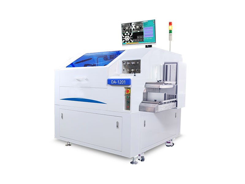
| Machine size and weight | Size | 2350x1570x1900mm(Length x Width x Height) |
| Weight | 1800kg |